Mark IIC (not IIC+) draft schematic

The Boogie Board

Help Support The Boogie Board:

This site may earn a commission from merchant affiliate links, including eBay, Amazon, and others.

chipaudette

Well-known member
Joined
Jan 19, 2009
Messages
330
Reaction score
2
Location
Vermont, USA
Hi All,

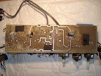
For the electrically inclined, I've made a first draft of the schematic for my Mark IIC (not IIC+). When I get around to sending it to Mesa to get it upgraded to the IIC+, we can compare the revised amp to this original to see what MikeB did to make the upgrade...

http://picasaweb.google.com/lh/photo/j3EcPGBg3Z_-iB4O92jBtQ?feat=directlink

Don't forget that you can click on "Full Screen" or "Download" to see the full size image.

If you check it out, you'll notice that there are some really large differences between the IIC and IIC+. I was quite surprised.

Chip
 
One of the unexpected features of the IIC schematic (assuming that I probed it out correctly) is that the main signal path comes off the cathode of V1B. This is different than any other Mark Series amp, where the signal is fed off the anode at the top. As a result, the gain of V1B is greatly reduced and the signal level going on to the rest of the circuit is lower than one would expect based on the other Mark amps. I'll say it again...this assumes that I've probed the circuit correctly.

If I did get it correct, this has implications on the lead channel. The IIC (and IIC+) were an innovation over the IIA and IIB by having two gain stages in the lead circuit. This should have made it more sensitive / higher gain. But, for the IIC, the lower-gain cathode-follower arrangement of V1B might eliminate much of the benefit of the two-stage lead circuit.

It's my opinion that the cathode-follower stage contributes almost no gain (it just buffers) so that, in effect, the IIC has a similar number of gain stages as the IIB. Based on this paper-only analysis of the schematics, I would think that it wasn't until the IIC+ went back to the anode of V1B that the full power of the two-stage lead circuit could be realized.

So, my question is, for those of you who have played both the IIC and the IIC+, does the lead channel of the IIC+ have significantly more gain and saturation available than the IIC? Asked another way, does the lead channel of the IIC feel like it has gain more like a IIB or more like the IIC+?

This is so fun!

Chip
 
I own a C and have never played a C+, but have heard many clips and read a lot of posts regarding the two versions. I also have a III and a IV. That said, IMO, the C has lower gain than the C+, III, and IV. The C is more in the Dumble catagory for gain. It's a great sounding amp for classic rock type music. The lead sustains great and is harmonically rich. But the C's lead can sound a little harsh. The lead really cuts through the mix and is much more "in your face" than the other Marks. From what I understand the C+ lead is smoother, which is closer to the III and IV's lean tone. The C's lead tone seems less compressed that the C+, III, IV.
 
Yeah,

I assume that it is 750p like all the other Marks...but I didn't want to put it on there if I couldn't see it or probe it. The Mark IIC had so many other surprises (like that effects loop) and I didn't want to make any assumptions.

So, inside the amp, the 250p treble cap and the assumed-to-be 750p shift cap are stuck together with a little hot glue (or whatever they use in the factory to stick together the tall components to reduce vibration). The markings on the treble cap are visible, but the markings on the other cap are covered up by the glue. Therefore, I couldn't confirm its value.

When I open up the amp the next time, I'll probably borrow a better DMM from my workplace so that I can probe the capacitance value in-circuit. Then I can confirm what we're all guessing to be true...that it's a 750p cap.

Chip
 
It's only in circuit when LDR1 is open. Reading in circuit, it's 1000pf treble circuit, plus the capacitance of the LDR and +/- 20% tolerance.
To further remove any assumption from your schematic, I would PM JVK. He has photos of the backside of the RP10. Their are traces for more than just the heaters.
 
Yeah, I'm a little worried about the in-circuit measurement. It's really tough to get a good measurement of a particular component when lots of other components are tied to it. Ideally, one would have switches or big resistors in place to isolate the component in question...

My thought was to do the test with the amp off. If I don't have the amp off, there will be a huge DC voltage across these caps, which would probably throw off my DMM. So, the amp will have to be off.

With the amp off, the LDR will be open, which will isolate one side of the cap from the rest of the circuit. That's good. Unfortunately, the other side of the cap will be exposed to a whole bunch of items: (1) the 250p treble cap followed by the 250K treble pot, (2) the 100K slope resistor followed by the bass and mid caps, (3) the anode of V1A and the guts of the tube, and (4) the 150K V1A anode resistor followed by the power supply rail and its giant 30u filter caps. Maybe those 100K+ resistors are enough isolation. I'm not hopeful. It looks like it'll be a pretty low-fidelity measurement.

Of course, the only reason that I can't read the caps value is that it's label is covered by the glue that's holding it to the neighboring cap. I could just pull the glue off the cap and take a look at its label. Then I could glue them back together and be done. That sounds like the best plan.

As for the seeing the backside of the board...man, that would be great. My schematic already includes a couple of traces that must be on the back based on my probing of circuit continuity with my DMM. I'd love to see if I missed any connections. It's hard to believe that I got them all. I'm looking forward to being corrected.

Also, any thoughts on how different the RP9 is from my RP10?

Thanks for you help!

Chip
 
Edit, I meant RP10. The RP9 was for the IIB. It's mot even close in comparison.
The LDR's with the amp off are in the off mode. They require voltage to the LED to open the photo resistor.
In the off mode, they have a 50 M? dark resistance for the 5C1 and 400 M? for the 5C4.

http://optoelectronics.perkinelmer.com/content/datasheets/dts_photocellanalogoptoisolator.pdf
 
Hi Again,

I opened up the amp AGAIN. I confirmed the 750p value on the treble shift by looking at it. I also corrected a few other values...

Mark IIC, Schematic V1.2:
http://picasaweb.google.com/lh/photo/yGt6WAvfw7LsCc0Nk1DQUw?feat=directlink

I also mapped out most of the EQ circuit and most of the power amp circuit. I'll draw that up this week.

Thanks for your interest!

Chip
 
Hello gentlemen. Here you go:

IIC+ pcb bottom


Word of caution... the level of butchery that I've performed here should only be practiced if you don't mind sacrificing the amp (partly at least), because you would be desoldering, cutting wires and/or damaging the pcb traces (amazing how easy the traces come off) on a 25 year old relic :)

All the best
Jonny
 
Hi Johnny,

Thanks so much for posting this pic. Unfortunately, when I click on it, I get an error from google...

The requested URL /_o912b1uGg_c/Sm0y8oTmN7I/AAAAAAAAABA/r2By-2Y06Q4/DSC02855.JPG was not found on this server.

Could you re-check your link? I'm dying to see the pic!

Thanks,

Chip
 
Hi All,

To anyone who still cares, I got a PM asking about my IIC (not IIC+) schematic. So, I dug it out again and saw that I had updated it without uploading it. So, if you want the latest version, the link is below. Note that there is now a page 1 (preamp) and a page 2 (power amp, EQ and a partial schem for the power supply). Enjoy!

Page 1: https://picasaweb.google.com/lh/photo/6SNBfcfYmpCM1ydhaRW1ANMTjNZETYmyPJy0liipFm0?feat=directlink

Page 2: https://picasaweb.google.com/lh/photo/9QM-EPHkmLAlrHPsJOHS8dMTjNZETYmyPJy0liipFm0?feat=directlink

Gallery: https://picasaweb.google.com/lh/photo/6SNBfcfYmpCM1ydhaRW1ANMTjNZETYmyPJy0liipFm0?feat=directlink


Chip
 
Chip, sadly the links with all your hard work are dead.

Do you think it might work better to attach them to a reply rather than using fickle external hosts?
 
RP10 IIC Schematic: https://drive.google.com/open?id=1mpJFsu2gHA2gIiNmg6FGbC81rlggkt6M
RP10 IIC Board View: https://drive.google.com/open?id=1Lx0AofY9eI34mGY3RbgNDSV5IgEUf5cS

RP11A IIC Schematic: https://drive.google.com/open?id=1_KWgnYKephAlJAnfH8IL9El8qHdo5nji
RP11A IIC Layout : https://drive.google.com/open?id=1CALqxt8hsJK_ghfb4ZnNmY8LQ627h54b

Based these on chipaudettes originals and expanded when I traced my RP10 IIC (original) fully. The RP11 is based off research but should be pretty much there 100%.
 
Back
Top